Photoelectric Proximity Switches in Sub-Miniature Technology
Contrinex 12th Dec 2022
Trend, requirements
For some time now there has been a marked trend towards smaller constructions of sensors. This is due to the increased demand for the automation of production processes, resulting in:
- a higher degree of automation;
- continuously controlled production quality at all production stages;
- low reject rate.
The purpose underlining these demands is mainly to improve the quality during manufacture and to reduce manufacturing costs. With regard to the sensor technology it means that, with basically unchanged criteria (e.g. machines, installations etc.):
- more and more sensors are installed and there is less and less space available for the installation of these sensors;
- sensors also have to be installed in almost inaccessible places;
- the demands for resistance against environmental influences (chemical, EMC etc.) are steadily increasing;
- installation of sensors by personnel not specifically trained in the installation must also be possible;
- it must be possible to exchange defective sensors quickly, simply and without reference to specialists.
All this combines to create an ever growing demand for small, powerful but nevertheless capable, robust and cost-effective sensors. With this situation in mind the following details will illustrate the process of developing a new line in photoelectric proximity switches and the results achieved.
Problematic situation
Cylindrical housings are preferred for smaller sensors. Sizes M18, M12 and M8 are at present available on the market for photoelectric equipment (versions in non-standard housings such as M6 and others with separate evaluation electronics are not discussed here). Required, but still not available, were units with a 4 mm diameter or with MS thread and which are known from inductive versions and used there in large numbers. The following text will describe the process adopted to realize this type of equipment.
Solution
The most straightforward solution to the problem and used in this case is to start with the technology employed for existing, larger units and to try to reduce the dimensions of the various modules.
The electronic unit
In order to reduce the size of the electronic module it is sufficient to use known processes (Chip-on-Board technology, SMD technology, extra-fine PCBs). It is, however, mandatory that always the smallest available components be used. The application of an integrated circuit combining the most important electronic functions is unavoidable.
The optical unit
Existing, larger versions are not suitable for reducing the optical unit.
This is due to a variety of reasons:
- There are no sufficiently small transmitter and receiver components (LED's and photodiodes) installed in housings.
- When using transmitter and receiver components in Chip form their surfaces, which transmit or receive light, are vertical to the required direction (Fig. 1).
- Lenses and deflector mirrors cannot be used for reasons of space.
- When using transmitter and receiver components in Chip form their surfaces, which transmit or receive light, are vertical to the required direction (Fig. 1).
- Lenses and deflector mirrors cannot be used for reasons of space.
In order to circumvent these obstacles a recognized optical component was used: the convex mirror. The divided or undivided version provides the desired solution. Fig.1 shows the construction of such an optical device as an example of the reflex light sensor.
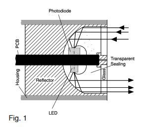
The light, either being transmitted or received, is diverted by 900 and bundled at the same time by the divided convex mirror plates. The required optical separation between transmitter and receiver is achieved through the interspaced PCB. By means of a suitable design of the PCB it is also possible to avoid the undesired electrical coupling between the two PCB layers.
EMC
In order to obtain sufficient EMC characteristics it is obviously necessary to effectively screen at least the receiver part of the unit (Photo diode and amplifier). However, with small components there really is no space available for the installation of shields. In order for the units to be suitable for use and to be authorized to carry the CE mark, they must demonstrate excellent EMC strength.
The convex mirror used is ideally suitable. In any case, it is preferably produced as a metal coated, plastic component. The desired EMC characteristics can be achieved quite simply by the electrical connection of the metal coating with a suitable point of the circuit and correct design of the PCB.
Environmental conditions
Good resistance against environmental conditions and influences is of paramount importance for problem-free use of sensors over a wide field of applications. Here the photoelectric equipment, in comparison with inductive equipment, has a definite physical disadvantage:
- The light path is negatively influenced by contamination;
- Contrary to other types of sensors, they cannot be sealed completely with casting resin. Even when using transparent resins their refractive characteristics have a serious and detrimental effect on the functions of light optics.
Here the new unit has decided advantages. By means of a suitable integrated circuit it was possible to include an excess light indication andIor an indication of contamination (in case of insufficient light reception the output state LED will flash). On the other hand, the optical system obtained with a convex mirror can be fully sealed with transparent resin without affecting its characteristics at all. It is well known that reflection is independent from the refraction index of the medium.
Construction and data
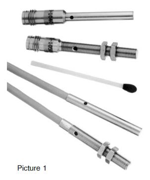
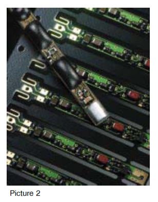
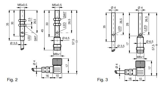
Examples of the equipment described is illustrated by Picture 1. The housings, with a diameter of 4 mm smooth or M 5 threaded, have a length of only 35 mm (cable version) or 57.5 mm (plug versions in plugged-in condition, including the plug). Picture 2 illustrates a view of the electronic module and Figs. 2 and 3 are scale drawings of the complete parts.
The equipment is completely sealed under vacuum with casting resin, without any form of air inclusions. Otherwise, in the long-term this could lead to reliability problems, e.g. through condensation. The light intake and exit surfaces are made from glass, so that they are scratch and solvent resistant (important for cleaning). The equipment does not contain any ceramic hybrid substrate and is therefore less liable to fracture.
The sensing ranges are 50 mm for the reflex sensor and 500 mm for the through-beam sensor. Short-circuit protection, all-round voltage reversal protection, over-voltage protection and switch-on pulse suppression is also incorporated. A LED signals the control state and insufficient light reception.
Technical data:
(according to IEC 60947-5-2)
Sensing range 50 I 500 mm
Supply voltage range UB 10 ... 30 VDC
Output current 100 mA
Current input 10 mA
Switching frequency 250 Hz
Switching times 2,5 msec
Max. ambient light:
incandescent 3'000 Lux
sun 10'000 Lux
Ambient temperature 0 ... + 55 0C
range
Protection class IP 67
EMC - protection:
IEC 60255-5 1 kV
IEC 61000-4-2 Level 2
IEC 61000-4-3 Level 3
IEC 61000-4-4 Level 2
Price
The selected processes permit cost-effective manufacture and therefore an attractive price. The costs are certainly less than, for instance, those for a fiber optic amplifier and the associated optical fibers.
Applications
The new photoelectric proximity switches have not been developed for specific applications. On the contrary, they were consciously designed as a universally adaptable unit for rough industrial use. As already mentioned, they satisfy the general trend and meet the requirements of optical systems. The subsequent information can therefore only reflect an incomplete selection of the many applications possible:
- Replacement for larger units with restricted installation space;
- Replacement for inductive units with insufficient sensing range;
- Installation in place of optical fibers. This would obviate the necessary and careful routing of the optical fibers. It is also a more economic solution to the problem of costs of optical fiber, fiber optic amplifier and their installation.
12th Dec 2022
